近日,昆明理工大学材料科学与工程学院陈江照教授团队和河北工业大学陈聪教授团队合作在国际材料顶级期刊Advanced Materials(IF=29.4)上以题为“Suppressing Ion Migration by Synergistic Engineering of Anion and Cation towards High-Performance Inverted Perovskite Solar Cells and Modules”发表最新研究成果,该研究工作得到国家自然科学基金面上、兵团重点领域科技攻关计划等项目的资助。
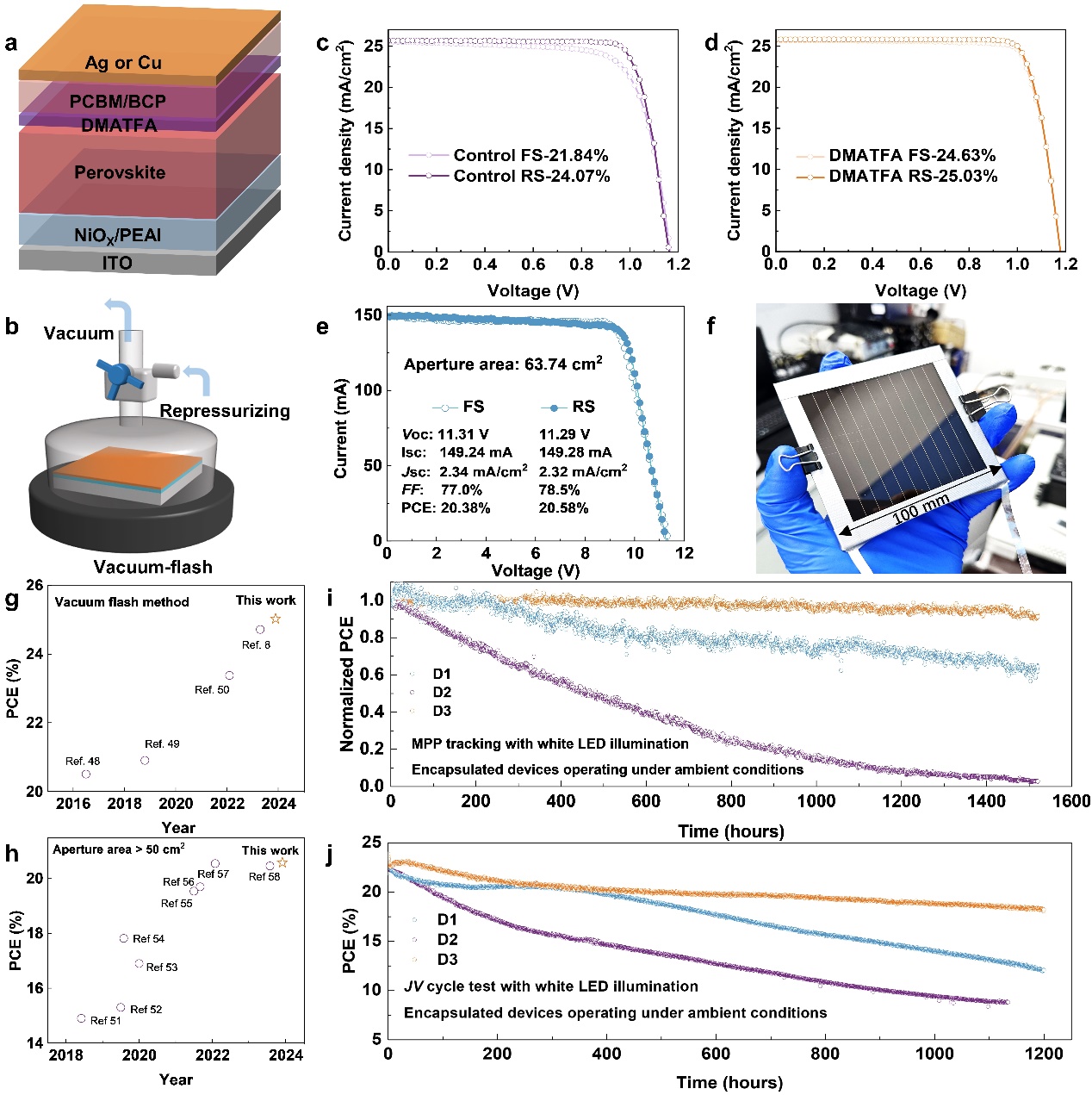
离子迁移引起的内在不稳定性和大面积制备对钙钛矿光伏技术的商业应用提出了严峻的挑战。鉴于此,昆明理工大学陈江照教授团队和河北工业大学陈聪教授团队合作开发了一种界面异质结和金属电极稳定策略,通过管理铅基缺陷来抑制离子迁移。在筛选了一系列阳离子和非卤素阴离子后,选择了由二甲基铵(DMA+)阳离子和三氟乙酸(TFA-)组成的理想有机盐分子二甲基三氟乙酸铵(DMATFA)来调控钙钛矿薄膜表面。DMA使活性过剩和/或未反应的PbI2转化为稳定的新相DMAPbI3,抑制了PbI2的光分解和离子迁移。同时,TFA-可以通过钝化未配位的Pb2+和/或碘离子空位缺陷抑制离子迁移。DMA+和 TFA-协同稳定异质结界面和银电极。基于DMATFA修饰的倒置钙钛矿太阳能电池和组件分别取得了25.03%(认证24.65%,0.1 cm2)和20.58%(63.74 cm2)的效率,这是迄今为止基于真空闪蒸技术的器件报道的最高效率。经过1520小时的最大功率点(MPP)连续跟踪后,DMATFA修饰的电池仍然保持初始效率的91%。

Figure 1. (a) Electrostatic potentials of EA+, Ace+, GA+ and DMA+. (b) The number of adsorbed EA+, Ace+, GA+, and DMA+ at temperatures of 300 and 400 K. (c) The adsorption energy between EA+, Ace+, GA+ or DMA+ and various acceptor-like defects. DOS of the Pb-I antisite surface (d) without and (e) with DMA+ treatment. (f) Binding energy of BF4-, PF6-, SCN- and TFA- at the surface of perovskite. The optimized structure of FAPbI3 (g) before and (h) after interacting with DMA+TFA-.

Figure 2. SEM images of the (a) control and (b) DMATFA-treated perovskite films. The (c) Pb 4f, (d) F 1s, and (e) C 1s XPS spectra for the perovskite films without and with DMATFA. GIWAXS images of the (f) control and (g) DMATFA-treated perovskite films. (h) XRD patterns of the control and 5 μL/mL DMATFA-treated perovskite films. (i) XRD patterns of PbI2, DMAI, and PbI2+DMAI films. (j) XRD patterns of PbI2, PbI2+MAI, PbI2+MATFA, PbI2+DMATFA+MATFA (molar ratio of 1:0.5:0.5), and PbI2+MATFA+MAI (molar ratio of 1:0.5:0.5) films.

Figure 3. Photographs of the (a) control and (b) modified PSCs after aging under one sun illumination and 85 ℃ for 120 h in nitrogen condition. PL mappings of the fresh (c) control and (d) DMATFA-treated perovskite films. PL mappings of the (e) control and (f) DMATFA-treated films after aging for 120 h under one sun illumination and 85 ℃ in nitrogen condition. Temperature-dependent conductivity measurements of the (g) control and (h) DMATFA-treated perovskite films. The activation energy (Ea) of ion migration was extracted based on the Nernst-Einstein relation. (i) The calculated Ea of I- migration in FAPbI3 and DMAPbI3. The inset figure shows the simulated I- migration process in FAPbI3 and DMAPbI3. TOF-SIMS for the (j) control and (k) DMATFA-treated devices after aging under one sun illumination and 85 ℃ for 120 h in nitrogen condition. Cross-sectional EDS mapping curves of the (l) control and (m) DMATFA-treated devices after aging under one sun illumination and 85 ℃ for 120 h in nitrogen condition. (n) TRPL of the control and DMATFA-treated perovskite films on the bare glass. (o) Dark J-V curves for the electron-only devices with the structure of ITO/SnO2/perovskite/PC61BM/Ag without and with DMATFA. The inset is the device configuration.

Figure 4. (a) The device structure of NiOx-based inverted PSC with DMATFA modification. (b) Device used for fabricating perovskite films based on vacuum flash technique. J-V curves of the champion (c) control and (d) DMATFA-treated devices. (e) I–V curve of the champion perovskite modules with DMATFA treatment. (f) Photograph of a DMATFA-treated perovskite module with substrate and aperture area of 100 cm2 and 63.74 cm2, respectively. (g) Comparison of the historical PCEs of the PSCs fabricated using vacuum flash technique8, 48-50. (h) Comparison of the historical PCEs of the PSC module with aperture area exceeding 50 cm2.51-58 (i) Continuous MPP tracking of the encapsulated PSCs under illumination with a white LED lamp (100 mW/cm2) without UV filter at 20 ± 2 °C and 30 ± 5% RH. The initial PCE of D1(the perovskite film with stoichiometric ratio), D2 (the perovskite film with 5% excess PbI2) and D3 (the DMATFA-treated perovskite film with 5% excess PbI2) devices is 23.04%, 23.98% and 24.87 %. (j) The J-V cycle test of the encapsulated control and DMATFA-treated PSCs under illumination with a white LED lamp (100 mW/cm2) without UV filter at 20 ± 2 °C and 30 ± 5% RH. The initial PCE of D1, D2 and D3 devices is 22.18 %, 22.34 % and 23.88 %.
文章链接:
Zuolin Zhang#, Mengjia Li#, Ru Li#, Xinmeng Zhuang#, Chenglin Wang, Xueni Shang, Dongmei He*, Jiangzhao Chen*, Cong Chen*. Suppressing Ion Migration by Synergistic Engineering of Anion and Cation towards High-Performance Inverted Perovskite Solar Cells and Modules. Advanced Materials 2024, 2313860.
https://doi.org/10.1002/adma.202313860

